Leave Your Message
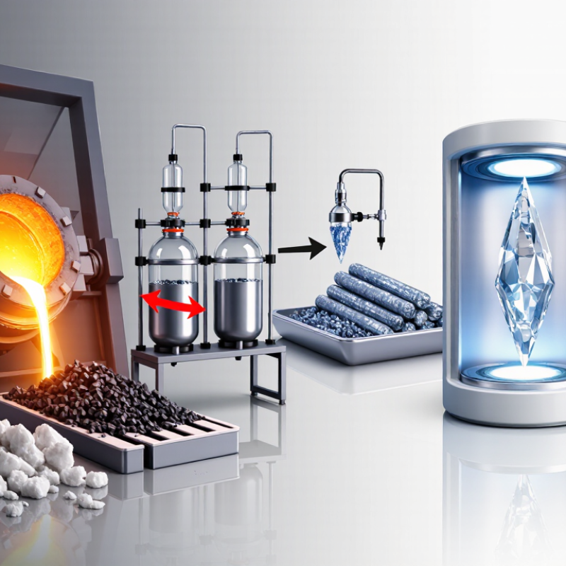
Quartz To Silicon describes a chain of heat, chemistry, and precise purification. It begins with quartz-rich material, usually processed to remove visible impurities. In a submerged-arc furnace, quartz reacts with carbon at very high temperatures, producing metallurgical-grade silicon. The gray, brittle output is not yet suitable for most semiconductor applications. That distinction matters.
Further refining removes impurities to produce high-purity polysilicon. Depending on the intended product, manufacturers may use processes such as the Siemens method or fluidized-bed deposition. Semiconductor-grade material then undergoes crystal growth, slicing, and wafer finishing. Each stage demands careful control; a tiny contaminant can affect electrical performance. Industrial details vary, and public descriptions do not always reveal proprietary operating conditions.
Gordon Moore, Intel co-founder and a central figure in semiconductor history, wrote, “It may prove to be more economical to build large systems out of smaller functions, which are separately packaged and interconnected.” His observation concerns integrated-circuit design, not quartz reduction itself. Still, it points to why the purity and consistency of silicon feedstock matter: later components depend on dependable materials. The process is powerful, but not perfectly tidy. Energy use, furnace emissions, and material losses deserve honest scrutiny alongside technical gains. Understanding Quartz To Silicon therefore means following both the chemistry and the manufacturing choices that turn mineral feedstock into electronic-grade wafers.
Quartz selection is the first quality control step in silicon production. Furnaces need consistent silica-rich feed, but iron, aluminum, boron, and phosphorus impurities can affect the final silicon. The USGS Mineral Commodity Summaries 2025 estimated world silicon production at 8.5 million metric tons in 2024, underscoring the importance of dependable feedstock at industrial scale. Clean-looking quartz is not always chemically clean.
At the quarry and receiving area, check representative samples for chemistry, grain size, moisture, and visible inclusions. Use laboratory assays suited to trace elements; a basic visual check cannot detect every contaminant. Quartz with dark veins, clay, or mixed rock may need rejection or extra sorting. Wash to remove dust and clay, then dry and crush the material to the furnace’s specified size range. Too many fines can hinder gas flow. Oversized pieces may heat unevenly. These details sound simple, yet they are easy to rush.
Tips: Keep a retained sample from each delivery. Record assay results and particle-size checks together; otherwise, a later furnace issue may be hard to trace. One caveat: the best-looking batch is not necessarily the best-performing one.
What Is the Quartz to Silicon Process? - Quartz Selection and Preparation for Silicon Production
| Stage or Dimension | What to Check or Do | Typical Guideline | Why It Matters |
|---|---|---|---|
| Quartz source selection | Assess quartz or quartzite deposits for consistency, mineral composition, and availability of suitable lump material. | Choose material dominated by quartz, with low clay, mica, feldspar, and iron-bearing mineral content. | Mineral impurities can add unwanted elements to the furnace burden and affect silicon quality and furnace operation. |
| Silica content | Test representative samples using a suitable chemical analysis method. | High-grade metallurgical feed commonly targets about 98–99% or more SiO2; the precise acceptance limit depends on the plant and product specification. | Silica is the silicon-bearing raw material reduced in the furnace. |
| Impurity analysis | Measure iron, aluminum, calcium, magnesium, phosphorus, boron, and other elements relevant to the intended silicon grade. | Keep impurity levels as low and consistent as practical. Phosphorus and boron may require specific limits when higher-purity silicon is intended. | Some impurities can transfer into the silicon, while others can influence slag formation, furnace chemistry, or downstream refining needs. |
| Physical integrity | Check lump strength, porosity, cracking, and resistance to thermal shock or decrepitation. | Prefer durable lumps that retain their size during handling and heating; verify performance with plant-relevant tests. | Excessive breakage creates fines, which can impair gas flow through the furnace burden. |
| Crushing and sizing | Crush and screen the quartz to the furnace’s specified lump-size range, removing oversize pieces and excess fines. | A commonly used starting range is roughly 10–100 mm, but the required size distribution is furnace-specific. | Consistent sizing supports stable burden permeability, heat transfer, and contact with the carbon reductants. |
| Washing and cleaning | Where needed, wash or otherwise remove adhering soil, clay, and loose mineral contamination; control the water and waste streams. | Use washing only when it effectively reduces surface contamination without introducing unacceptable residues or excess moisture. | Removing surface contaminants can improve feed consistency and reduce unwanted material entering the furnace. |
| Drying and storage | Drain and dry prepared quartz as required, then store it separately from soil, dust, and other raw materials. | Maintain moisture within the plant’s handling and furnace-feed limits; prevent recontamination during storage. | Moisture affects handling and introduces additional water vapor into a high-temperature process. |
| Sampling and quality control | Take representative samples from each lot and record chemistry, size distribution, moisture, and physical condition. | Set acceptance limits and sampling frequency according to feed variability and the required silicon grade. | Routine checks help maintain a consistent furnace burden and identify changes in the quartz supply. |
| Furnace reduction context | Blend prepared quartz with carbonaceous reductants and charge the mixture to a submerged-arc furnace. | At high furnace temperatures, silica is reduced to silicon; carbon monoxide is produced as a reaction gas. | Quartz preparation is one part of the overall process, alongside reductant quality, burden design, furnace control, and subsequent refining. |
The values shown are general process guidelines, not universal purchasing specifications. Actual quartz limits and size distributions should be set for the specific furnace, operating practice, and silicon product.